JTAG - Joint Test Application Group
- Its used for verifying design and testing PCB after manufacturing
- Its referred as IEEE Standard 1149.1
- Standard Test Access Port and Boundary-Scan Architecture
- Programming and debugging both can be done using JTAG
Physical interface:
- Its used for verifying design and testing PCB after manufacturing
- Its referred as IEEE Standard 1149.1
- Standard Test Access Port and Boundary-Scan Architecture
- Programming and debugging both can be done using JTAG
Physical interface:
- TDI (Tets Data In)
- TDO (Test Data Out)
- TCK (Tets Clock)
- TMS (Test Mode Select)
- TRST (Test Reset)
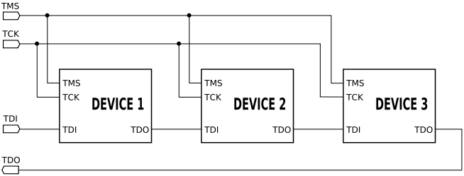
Daisy chain way of using JTAG
SWD - Serial Wire Debug
Serial Wire Debug (SWD) is debug port for microcontroller where package is small, or small number of pins.
Its used mostly in ARM architecture chips
SWD is availabel as a part of Core Sight Debug access port
Compatible with all ARM processors, and any processor that uses JTAG
- Programming and debugging both can be done using SWD
- Programming and debugging both can be done using SWD
Physical interface:
- SWCLK (Serial Wire Clock)
- SWDIO (Serial Wire Data In and Out)
In case when SWD is used for JTAG based process
- SWCLK --> TCK
- SWDIO --> TMS
With SWD protocol, the debugger is connected to AMBA bus as another master, using which debugger can access ARM core system and peripheral memory
NOTE:
Ofcourse, VCC and GND need to be common between In-Circuit-Debugger/Programmer and Processor
SWO (Serial wire out) wire is used sometimes along with SWCLK and SWDIO.
Some of the programmer and debuggers like STLINK provide debugging utility like printf(), which are very useful. These utilities use SWO wire to send serial data over it to PC. But here you need to set the system clock value correctly in the serial debug viewer configuration on PC.
debugWIRE
debug WIRE is a single wire interface provide in most Atmel AVR microcontrollers.
Its even more beneficial compared to JTAG and SWD as its very useful in places where package pin count is very small. On-Chip-Debugger (OCD) is provided on silicon itself by Atmel. dW single wire is internally connected to OCD. Whenever BREAK instruction (Software breakpooint) or (Hardware breakpoint) is observed by OCD, the CPU core operation is stopped and halted. All the SRAM, Peripheral register values, IO status information is sent by OCD over dW wire to the External Debugger unit(JTAGICE3). It will convert dW information to USB so that information could be sent to PC. On PC there will be a Debug software program which will grab the data and display it. Debug software running on PC will be a part of AtmelStudio.
- Only debugging both can be done using debugWIRE
- SPI interface is used for programming where dW debug interface is used

Physical interface:
Single wire dW.
Its a alternate functionality for RESET pin of the micro controller.

No comments:
Post a Comment